Cooled CCD cameras have long been at the forefront of astrophotography. But what really is CCD sensor technology, and how do we use it to create stunning images of the night sky?
We thought it might be useful to take a look at some of the different aspects of CCD sensors to help provide a better understanding of what’s happening on the surface of your camera while you’re busy imaging the universe.
We’ve put together a few videos in this series that we’ll release over the coming weeks, including a look at the different types of noise associated with CCD sensors and how we go about minimising it. But let’s start at the beginning and take a look at what a CCD – or charge coupled device – actually is.
What is a CCD? – Transcript
Hello.
What I’d like to do today is talk a bit about CCDs themselves. CCDs obviously have been really important for astrophotography over the last ten or twenty years – most of the really great images of the night sky have been taken with CCD sensor technology. So what we’re going to do here is take the opportunity to talk a little bit about the sensors themselves. Hopefully this will be informative, it may be entertaining. It’s probably not going to be particularly useful in terms of helping you take a picture of the night sky, but when you want to have an idea of what’s actually happening on the camera itself, it may be useful.
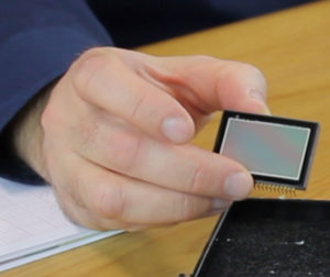
Okay, so this is a sensor. It’s actually one of the Kodak eleven megapixel sensors, and it looks similar to some of the Sony sensors, in as much as that we have a clear piece of cover glass covering a piece of silicon chip itself and we have a number of pins along the side – or it can be a pin grid array – to actually communicate with the electronics outside.
- Kodak 11MP sensor
- Pin Grid Array
The first thing to actually note is it’s a piece of silicon. So why on earth have we got a piece of silicon chip under there? Why have we chosen to use that, why haven’t we chosen to use a piece of steel, or a piece of coal, or plastic – why silicon? And the answer really comes down to a very interesting property of silicon and to kind of talk you through that, it’s useful to talk about a number of different types of compound and their electronic properties.
Types of Compound and Their Electronic Properties
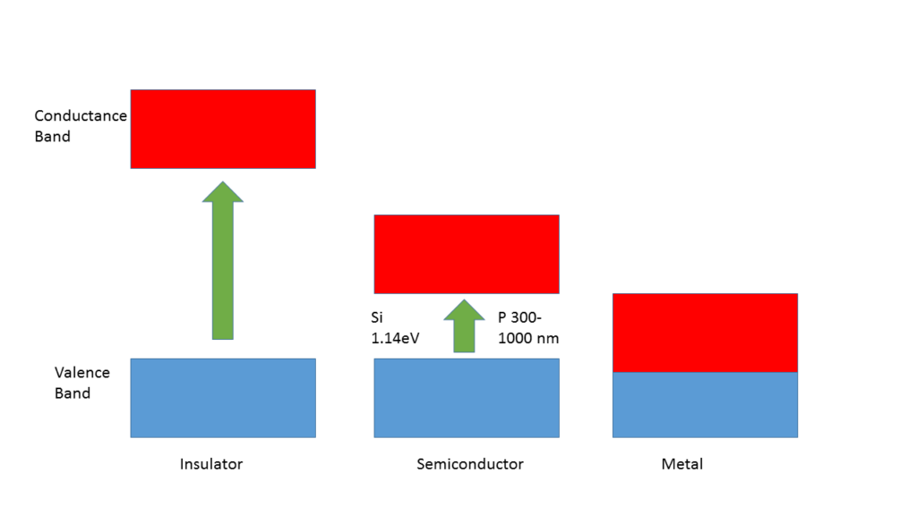
An insulator is a material where all the electrons are in the valence band, so they’re bound closely to the parent atoms and they can’t move around the material at all. Electrons that are delocalised that can move are what’s called in the conductance band. Insulators do have a conductance band, but their energy is so much higher than the valence band that it’s very, very seldom that an electron will get promoted into the conductance band, and then it’ll tend to fall straight back to its parent atom and be bound. So insulators – very poor at conducting electricity.
In metals we have the converse situation where the valence band and conductance band energies actually overlap. So we have this sea of delocalised electrons within the metal and that helps it to conduct electricity, and that can do that without actually adding any energy into the metal itself.
Our third type of material, the semiconductor, has this interesting property where the conductance band is only slightly above the valence band, so we have to add a relatively small amount of energy in order to promote electrons into the conductance band. For silicon, that energy is 1.14 electron volts and the interesting property there is that corresponds to the amount of energy that a photon has between 300-1000 nanometres. That energy can be used if a photon falls onto the silicon, then it can be used to actually promote an electron into the conductance band and there, once it’s in the conductance band, we can then move it around the silicon and measure it.
Creating a Silicon Sensor
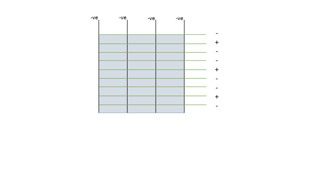
Okay, so now I’d like to consider how we actually design an image sensor around a piece of silicon chip. So here I’ve just got this on screen representing a square piece of silicon. I’m going to chop this up into nine areas which become nine pixels. The first thing to do is to separate the columns, so we put these stops in between the columns and these are basically little electrodes that run across the surface of the chip and they carry a negative charge, or we give them a negative potential and it stops any electrons that have fallen within these three different areas now migrating left and right across the sensor.
- Piece of Silicon
- Add pixels
- Add electrodes
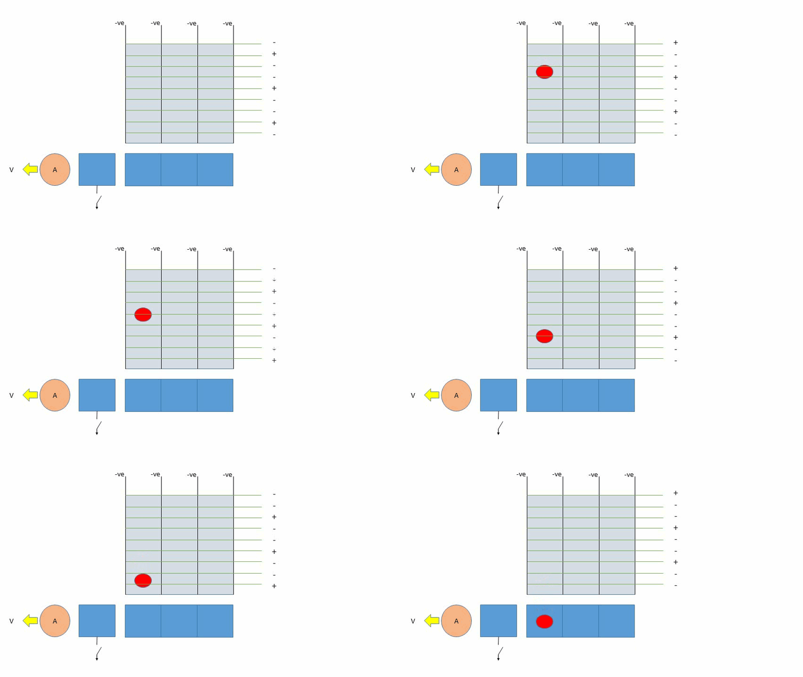
So that’s constrained them left and right. We also need to constrain them up and down and we use these vertical clocks in order to do this. So here they’re running in groups of three, so three clocks per pixel, and at the moment I’ve got the middle one with a positive potential, and the two outside ones with a negative potential.
So what happens now is if a photon was to fall onto one of these pixels, it’s going to generate and liberate an electron and that electron is going to want to move so it’s underneath the positive potential of the positive clock. This is the way it accumulates an image, so during the exposure time we have photons falling on the image sensor and they’re constrained within the pixel by the vertical electrodes and these horizontal-running vertical clocks.
- Vertical Clocks
Reading Out an Image
Then we want to read out that image. The way we do it is by actually clocking those vertical clocks.
If we move the potential of the clocks down one, so the positive potential has moved down one clock, what it tends to do then is to move, or to ask, the electron to migrate one stage at a time. And again, we do it by moving the positive phase down one and the electrons slowly migrate down the CCD itself.
We carry on doing this until the electrons, or the pixel, will transfer into the bottom stage which is this horizontal readout register. This is exactly the same kind of thing, but this time the clocks themselves are running vertically and so they allow to move the electrons left to right. So in this case we’re moving them over towards the left and into the final stage. And once they’re in that stage, we’re using an amplifier and the amplifier basically measures the number of photons that were loose in the pixel and converts it into a voltage, and that voltage then appears on one of the pins on this chip itself. On this one I think it’s one from the end – so one side’s vertical clocks and one side’s horizontal clocks.
Then when we’ve finished measuring that, or digitising that particular voltage from that pixel, we use the switch in the output stage to clear all the charge away from that pixel and clock one more of the horizontal registers into the output gate.
- Reading out a CCD
So a very typical system to readout a CCD is first of all, one line at a time into the horizontal readout register, then moving that one pixel at a time into the output stage. And this describes really what is a very classic area sensor for CCDs. It’s quite an old technology, quite an old way of handling, or using silicon, to become an imager. It does need a mechanical shutter, so during the readout stage, the whole thing is still sensitive to light, so in order that when you start to move an image down the sensor you don’t get trailing, you do need to use a mechanical shutter.
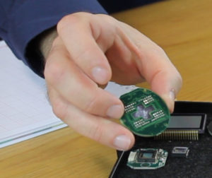
All of the sensors on this particular tray are not area sensors, they’re actually all interline sensors. A lot of our products within the Atik range use interline sensors that don’t need mechanical shutters. So it’s probably worthwhile just touching on how we go about using those.
Interline CCD Sensors
So, if we start off with exactly the same piece of silicon again and this time we’ll make it into an interline sensor, the first thing to do really is to start by making the same area-type sensor. So I haven’t shown them here but we’ll introduce these vertical column stops to stop the electrons migrating left and right and we’ll have the vertical clocks as well that allow us to move charge up and down the pixel itself.
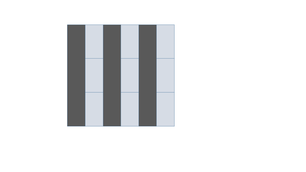
Where things get different is we put these bands of aluminium on top of the sensor itself. These basically make the area underneath the aluminium light shield insensitive to light, so during the readout phase, if there are any electrons within that part of the readout register, then as they’re being moved down the column, we don’t have to worry about that part of the sensor picking up further photons and converting them into electrons – there’s this light shield on top of them.
- Sensor with Aluminium Light Shields
We also now need something to actually be sensitive to light. In this case it’s called a photodiode, exactly the same idea, it’s a piece of silicon, except we’ve got a couple of other clocks we can now use to control this photodiode. One of them we can use to clear the charge from all the photodiodes in one go, and that’s typically used at the start of an exposure, and the second is a clock that’ll move the charge from all the photodiodes over towards the left here. That will then basically move them underneath the aluminium light shields and will effectively then end the exposure.
So this is basically a diagram of what an interline sensor looks like, because we’ve got a photodiode and we’ve got the vertical readout CCD underneath an aluminium light shield.
Where this isn’t very good is now what we’ve done is we’ve made the area of the sensor itself that’s sensitive to light that’s only about 25% of the surface of the chip. We’d describe that as having a fill factor of around 25% which is pretty bad if we’re looking at a low light source because 75% of the photons falling on that sensor aren’t going to be converted into electrons.
Adding Microlenses
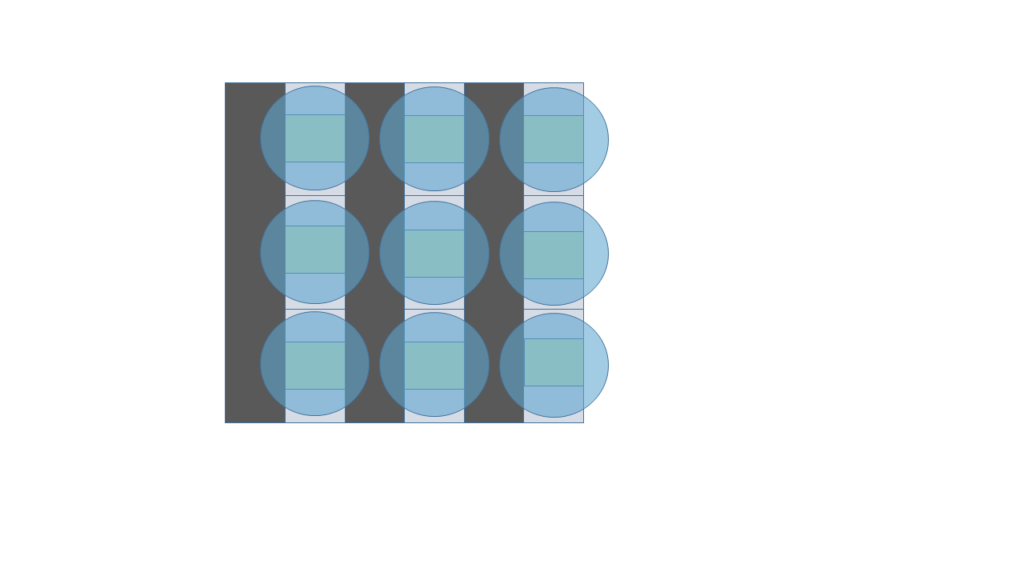
Here’s where things get clever again. The chip manufacturers introduce this microlens technology, so on top of each photodiode we put this lens, or they put the lens on top which means any photons now falling on top of the lens get concentrated onto that photodiode itself, and that will then improve the fill factor up beyond 80%.
- Interline Sensor with Microlenses
The technology they use to actually produce these very, very tiny lenses has been through a lot of development and is relatively interesting in itself. It’s usually an inkjet type process, where these little lenses are spotted one at a time onto the sensor surface. But then they take up more of a round spherical kind of shape when you do that, so then to actually get them back into a lens shape, the chip is controlled with some very careful temperature gradients to get these balls to sag into the shape of a lens. Once they’ve done that, then the fill factors effectively go up because of the microlensing.
Okay, I think that’s given as much as I probably want to talk about in this little section on CCD sensor. I hope it’s been interesting, and maybe when next time you’re out imaging the skies, as well as pondering the intricacies of galaxies and nebulae, we can also start to think about what’s going on actually on the sensor surface.
Thank you.

